
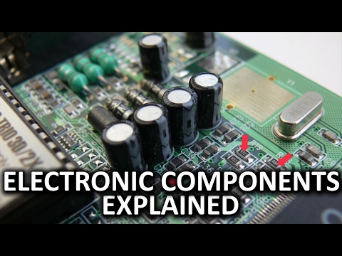
The printed circuit board (PCB) meeting course of consists of various steps and pointers that must be performed in the proper sequence for the finished product to operate as designed. To make sure that this occurs, PCB manufacturers use display screen templates and controlled heating and cooling mechanisms to regulate how parts are applied and fastened into place. While you assemble a printed circuit board, you must choose the right expertise for the type of components at hand. The entire elements and items should be correctly aligned of their designated spot, as specified within the PCB design. Any deviation, ever so slight, can have enormous ramifications on the features of the finished board. Substrate: The foundational material of the printed circuit board, the substrate makes every board agency and inflexible. Copper: Each working facet of a PCB contains a skinny layer of copper, for conductive functions. On single-layer boards, copper is positioned on the energetic side. On double-sided PCBs, copper appears on both sides.
Solder mask: This is the layer at the surface (typically inexperienced) of each printed circuit board. Solder mask offers insulation between copper and other supplies, preventing shorts that could in any other case happen if different conductive materials come into contact. Solder mask offers structure for the format of the PCB by keeping everything in its place. Each board incorporates holes that go through the solder mask. Solder is placed within each hole, which gives a basis for every element that gets added to the board. Silkscreen: The final touch on each printed circuit board is the silkscreen, a transparent layer that displays numbers and letters subsequent to the different parts of a given board. This enables manufacturers to identify the particular components of each board. Manual soldering: This is a process the place a technician manually inserts a single component onto its designated spot on a sequence of printed circuit boards. Once completed, every board is shipped to the next technician, who adds another half and passes the board onward.
Wave soldering: Wave soldering includes correctly soldering the place the board is placed on a conveyor and run via a heating chamber. Here, a wave of solder is applied to the bottom, fastening all the underpins of the board into place in a single course of. Additionally it is vital to understand the differences between by way of-hole, floor mount and mixed know-how assemblies. Through-gap expertise is the best selection for printed circuit boards that feature leads or wires that are threaded by means of holes within the board and then secured on the other aspect with solder. PCBs with large parts are especially suited to by means of-gap technology, especially capacitors. 1. The technician manually assembles parts onto specific areas on a printed circuit board, in keeping with the design specs of the PCB. Each element must be set in an actual position, as specified, for the PCB to operate properly. 2. The board is examined to ensure that all the elements have been properly assembled and that every part is ready in its precise place.
If any of the PCB components are misplaced, now could be the time to right these imperfections. 3. The components are actually soldered into place on the circuit board. This is usually achieved with wave soldering, the place the board strikes above a wave of hot solder liquid which solidifies the PCB assembly. This will also be finished by hand or by utilizing selective solder. Selective solder is similar to wave soldering, nevertheless, the operator can solder areas selectively and this helps whenever you don’t want solder on certain areas. Through-hole boards sometimes contain parts with wire leads, both axial or radial. Compared to surface mount technology, by means of-hole boards generally characteristic stronger bonds. However, extra work is required to provide a through-gap meeting because of the additional drilling concerned. If a through-gap board consists of multiple layers, sign traces have restricted routing on the internal layers as a result of the holes reduce by means of between the top and backside surfaces.
Therefore, by means of-gap expertise is often restricted to some of the bulkier PCB components like electrolytic capacitors and semiconductors. Boards that require extra firmness and support, akin to electromechanical relays and plug connectors, are also made with by way of-hole technology. In the course of the prototyping stage, technicians typically favor the larger by-gap to the surface mount because the previous works extra readily with breadboard sockets. However, if a board is intended for top-velocity or high-frequency functions, the design may require floor mount know-how to cut back stray reluctance. Otherwise, the function of the circuits could be degraded due to inductance or capacitance in the leads. If you loved this information and you would such as to obtain more details pertaining to pcb board (https://www.metooo.io/u/655b7a5e9db0d335ebe7aa4f) kindly browse through the web site. During the application of solder paste, a solder stencil is positioned on prime of the printed circuit board to ensure that the solder stays within the boundaries specified in the design. The stencil is a thin replica of the unique design with cutouts for the areas the place the parts are positioned.